Resistance size and resistance packaging
The resistor has a variety of different packaging styles and sizes. The most commonly used today is the rectangular surface paste (SMD) resistor, but the ancient axial resistor is still widely used in the design of the hole. This page provides information about SMD, axial and MELF packaging dimensions. It also provides some recommended pads for SMD components for welding to PCB.
SMD resistor size
The shape and size of the surface -sticker is standardized, and most manufacturers use the JEDEC standard. The size of the patch resistance is represented by the digital code, such as 0603. This code contains the width and height of the package. Therefore, the British code 0603 represents 0.060 "and the width is 0.030."
SMD packaging code can be given by British or public units. Generally speaking, British code is more commonly used to represent the packaging size. It is confusing that even if the British naming agreement is used, the public size is often used during the design of the printing circuit board (PCB). Generally, you can assume that the code is expressed in the British unit, but the size used is in millimeter. The size of the SMD resistor used mainly depends on the required rated power, the minimum feature size of the PCB manufacturing, and the restrictions of the equipment. The following table lists the size and specifications of commonly used surface packaging packaging.

| code | length (L) | width (width) | height (h) | power | ||||
| empire | public system | inches | mm | inches | mm | inches | mm | tile |
| 0201 | 0603 | 0.024 | 0.6 | 0.012 | 0.3 | 0.01 | 0.25 | 1/20 (0.05) |
| 0402 | 1005 | 0.04 | 1.0 | 0.02 | 0.5 | 0.014 | 0.35 | 1/16 (0.062) |
| 0603 | 1608 | 0.06 | 1.55 | 0.03 | 0.85 | 0.018 | 0.45 | 1/10 (0.10) |
| 0805 | 2012 | 0.08 | 2.0 | 0.05 | 1.2 | 0.018 | 0.45 | 1/8 (0.125) |
| 1206 | 3216 | 0.12 | 3.2 | 0.06 | 1.6 | 0.022 | 0.55 | 1/4 (0.25) |
| 1210 | 3225 | 0.12 | 3.2 | 0.10 | 2.5 | 0.022 | 0.55 | 1/2 (0.50) |
| 1812 | 3246 | 0.12 | 3.2 | 0.18 | 4.6 | 0.022 | 0.55 | 1 |
| 2010 | 5025 | 0.20 | 5.0 | 0.10 | 2.5 | 0.024 | 0.6 | 3/4 (0.75) |
| 2512 | 6332 | 0.25 | 6.3 | 0.12 | 3.2 | 0.024 | 0.6 | 1 |
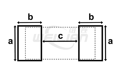
Puppet pad pad pattern
When designing the surface paste components, the correct pad size and pad pattern should be used. The following table shows the recommendation size of the pad pattern of common surface installation packaging. The following table lists the size of the return welding. For wave welding, use smaller pads.

| code | pad (a) | pad (b) | gap (c) | ||||
| Empire | Public System | inches | millimeter | inches | millimeter | inches | millimeter |
| 0201 | 0603 | 0.012 | 0.3 | 0.012 | 0.3 | 0.012 | 0.3 |
| 0402 | 1005 | 0.024 | 0.6 | 0.020 | 0.5 | 0.020 | 0.5 |
| 0603 | 1608 | 0.035 | 0.9 | 0.024 | 0.6 | 0.035 | 0.9 |
| 0805 | 2012 | 0.051 | 1.3 | 0.028 | 0.7 | 0.047 | 1.2 |
| 1206 | 3216 | 0.063 | 1.6 | 0.035 | 0.9 | 0.079 | 2.0 |
| 1812 | 3246 | 0.19 | 4.8 | 0.035 | 0.9 | 0.079 | 2.0 |
| 2010 | 5025 | 0.11 | 2.8 | 0.059 | 0.9 | 0.15 | 3.8 |
| 2512 | 6332 | 0.14 | 3.5 | 0.063 | 1.6 | 0.15 | 3.8 |
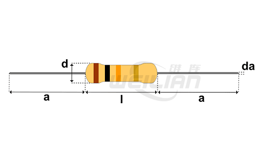
Axial resistor size
The size of the axial resistance is not as standardized as the patch resistance, and the size often used by different manufacturers is slightly different. In addition, the size of the axial resistor depends on the type of the rated power and the resistor, such as carbon ingredients, winding, carbon membranes, or metal membranes. The figures and forms below and forms are given the size of common carbon membranes and metal membrane axis resistors. Whenever you need to know the exact size, be sure to view the manufacturer data table of the component.

| Rated power | body length (L) | Vallest diameter (d) | Drawing length (a) | Diger diameter (DA) |
| tile | millimeter | millimeter | millimeter | millimeter |
| 1/8 (0.125) | 3.0 ± 0.3 | 1.8 ± 0.3 | 28 ± 3 | 0.45 ± 0.05 |
| 1/4 (0.25) | 6.5 ± 0.5 | 2.5 ± 0.3 | 28 ± 3 | 0.6 ± 0.05 |
| 1/2 (0.5) | 8.5 ± 0.5 | 3.2 ± 0.3 | 28 ± 3 | 0.6 ± 0.05 |
| 1 | 11 ± 1 | 5 ± 0.5 | 28 ± 3 | 0.8 ± 0.05 |
Mell resistor packaging size
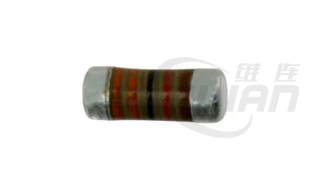
Metal electrode -free surface (MELF) is another surface -packed resistor packaging. The main advantage of using MELF instead of standard SMD packaging is lower thermal coefficient and better stability. The resistance temperature coefficient < / u> The film MELF resistor (TCR) is a TCR that often has & gt; 200 30ppm / k. The lower TCR of the MELF resistor is due to their cylindrical structure. This cylindrical structure also brings obvious disadvantages to the packaging, mainly because the module must be used to place components. Because they are round, special suction cups and larger vacuum are needed.
There are three common Melf packaging sizes: Micromelf, Minimelf, and Melf. The following table lists these types of characteristics.

| Name | abbreviation | Code | length | Diameter | Power |
| millimeter | millimeter | tile | |||
| Micro MELF | Mobile Management Unit | 0102 | 2.2 | 1.1 | 0.2 — 0.3 |
| Mini MELF | Comprehensive Fighting | 0204 | 3.6 | 1.4 | 0.25-0.4 |
| Merff | MMB | 0207 | 5.8 | 2.2 | 0.4 - 1.0 |

